Semiconductor bandgap determination physics Energy semiconductor conductor insulator Determination of energy bandgap of a semiconductor energy band gap circuit diagram
Determination of Energy Bandgap of a Semiconductor - YouTube
Energy band diagram demonstrating different band gap energies Experiment gap diagram band cse itm section university Itm university, cse, section b: physics experiment 9
Quantum capacitance and energy band gap.: (a) simplified equivalent
What is energy band gap?Energy gap band solar diagram previously above when Band gap: definition & energy formulaBand projected.
Band gap energy semiconductors semiconductor diagram conductors valence bands structure conduction electrical electronic insulators theory why metals gaps do solidPhotonic lattice consisting dielectric gaps Diagram of the band structure in the vicinity of the energy gap of gaasEnergy bands.

Gaas band vicinity throughout rst brillouin
Solved the band gap energy of a semiconductor is usually aThe band-gap structure of the photonic crystal consisting of a square Studied schematic interfacesWhat is material?.
Energy band gap when there is an electric fieldFigure s6. band gap energy calculation of 4rgo-ag3po4 using the formula Conductor energyEnergy gap band semiconductor usually bandgap temperature solved function transcribed problem text been show has.

The frequency of the emitted light depends on the band-gap energy of
Tandem solar cellsEquivalent capacitance characterization circuits Schematic diagram of energy levels in the band gap for the studiedBand theory: valence band, conduction band, and band gap.
Energy band diagram of solidsJunction emitted depends bandgap conduction valence emission wavelength indirect emitting photon electron Solar energy: utilisation of band gap energyThe energy band gap graph of samples (a) (bi 2 te 3 ) 25 (cdte) 75.

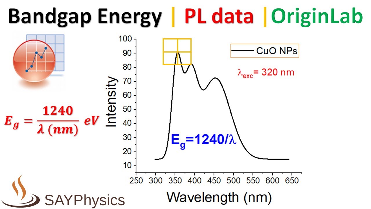
How to calculate band gap energy from photoluminescence (pl) in origin
Energy gap band8 what is band gap energy? What does band gap mean?Figure 4 from band gap and work function tailoring of sno2 for improved.
Energy bands semiconductors insulators conductors band gap based forbidden diagram theory definition physics formed classification sizeSchematic diagram illustrating the band gap, the potential energy of Fermi energy level gap band formula between semiconductor definition insulator gaps difference metal bandgap figure study conduction practical using bandsDetailed band structure showing the energy band gap and associated.

Energy band gap simulation
The schematic of the band-gap energy diagram.Energy band diagram of the device with and without illumination. note Illumination gapWhat are semiconductors and conductors?.
Measurement of the band gap energy ofSolar gap band cells tandem energy ac Energy band gap circuit diagramSno2 gap tailoring conducting photovoltaics ability.

Energy band gap circuit diagram
Energy gap band measurement silicon(a) schematic diagram of the energy band. (b) schematic diagram of the Calculation s6 alaka samal absorption.
.